Language
Ultra-High-Speed Optical Transceivers and Core Components
Release Date:2026-03-26
By Shen Bailin
Ultra-high-speed coherent optical transceivers are core components of full-band OTN networks, and their rates, transmission distances, power consumption, and costs directly affect the evolution of the optical transport network infrastructure. At present, long-haul 400G and metro 800G are in commercial deployment phase, and long-haul 800G and metro 1.6T are in technical development phase. When the single-wavelength rate increases, the working band needs to be extended to support the upgrade of the single-fiber transmission capacity. For example, the working band of the 400G long-haul coherent optical transceiver extends from the C band to the C+L band, and the T-bit long-haul coherent optical transceiver may evolve to the S+C+L band in the future. With the advancements in coherent optical transceivers, core components are facing challenges in bandwidth, integration, power consumption, and cost, and are driving innovation in new materials, new architectures, and new packaging processes.
Development Status
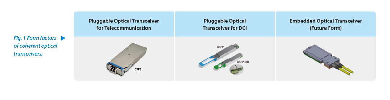
Coherent optical transceivers for long-haul and metro transmission in the telecom field are mainly CFP2. Coherent optical transceivers for interconnection between data centers are available in QSFP-DD and OSFP form factors. Optical transceivers have traditionally been required to be standardized, small factor, pluggable, and easy to maintain. ZTE uses CFP2 coherent optical transceivers. Below is an overview of the technological status of coherent light sources and optical components in an optical transceiver.
Coherent light sources include integrated lasers and external-cavity lasers. The monolithically integrated InP laser does not support C+L integration. External-cavity lasers consist of two solutions: spatial optical filters and silicon photonic filters. The wavelength dependence of the high-reflection film in the etalon of the spatial optical filter solution makes it difficult to achieve C+L band integration. ZTE's coherent light source solution is a Nano-packaged external-cavity laser. It employs a silicon photonic filter design and utilizes an innovative structure combining dual micro-rings and a Mach-Zehnder interferometer, shaping the resonant notch and suppressing the competing mode peaks. The laser frequency tuning range can be extended to 12 THz, covering 240 wavelengths across the integrated C+L band. This represents a twofold increase compared with the tuning range of the current mainstream C120/L120 solution in the industry. The laser achieves a linewidth of 30 kHz, meeting the requirements for long-haul transmission systems.
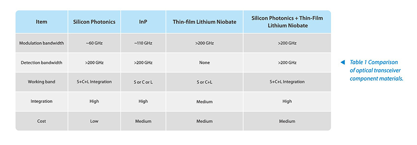
Coherent optical transceiver components are mainly made of silicon photonics, InP, and thin-film lithium niobate. Silicon photonic components offer significant cost advantages. They use wavelength-independent designs such as adiabatic couplers, supporting C+L integration, but have limited modulation bandwidth. In the future, silicon photonics will evolve toward the integration of thin-film lithium niobate materials to support large-bandwidth modulation.
InP components offer large bandwidth but are costly. A key advantage is the ability to integrate semiconductor optical amplifiers (SOAs) to achieve high power output, while the wavelength-dependent loss introduced by the multi-mode interferometer in the modulator can be compensated by the SOA. For C+L integrated InP components, it is necessary to overcome the technical challenges of amplification across the C+L band in SOAs and to improve the wavelength-related phase performance of the 90° optical hybrid in the receiver.
Developed from bulk lithium niobate, thin-film lithium niobate supports C+L integration by utilizing a multimode interferometer with low wavelength sensitivity. ZTE uses a technology platform based on silicon photonic receivers and thin-film lithium niobate modulators, enabling the realization of C+L integrated 128 GBd optical transceivers through packaging integration.
Future Evolution
C+L integrated optical transceivers have become a clear market requirement. To support the evolution of optical transceivers towards ultra-high speeds, technical innovations are required in the electrical interface form factors, materials for optical transceiver components, and component packaging technologies.
In terms of optical transceivers, pluggable optical transceivers are expected to remain the mainstream until 2030. As the single-channel electrical signal rate on the board increases to 448 Gbps and beyond, the form factor evolution of optical transceivers may follow two directions: introducing flyover cables or co-packaged cables (CPC) to improve the quality of electrical signal transmission while supporting front-panel pluggable transceivers, or embedding optical transceivers within a board, where coherent optical transceivers are placed as close as possible to the digital signal processing chips, as shown in Fig. 1. The power consumption of coherent optical transceivers increases in a spiral manner, and advanced heat dissipation technologies such as cold plate liquid cooling will be gradually introduced. The driving force of optical transceiver rate evolution is to increase the baud rate and reduce the number of optical and electrical channels, lowering the transmission cost per bit. When the optical baud rate reaches 400+ GBd, the dual-wavelength parallel architecture may be used to meet higher-rate transmission requirements in consideration of cost performance.
As the demand for high bandwidth in photonic integrated chips grows, research into new optical transceiver materials is increasing. These materials, including lithium tantalate, barium titanate, and graphene, have high electro-optic coefficients. The application of these materials should offer advantages in cost or performance. Based on the silicon photonics technology, the integration of new materials to complement each other’s strengths represents a crucial direction. The characteristics of optical transceiver component materials are shown in Table 1.
 Heterogeneous integration of silicon photonics and thin-film lithium niobate may become the mainstream technology for coherent optical components in the future. It supports S+C+L integration and the 400+ GBd baud rate required by 2030. The silicon photonic passive components at the transmitting end support multi-band operation, while the thin-film lithium niobate waveguide is used solely for modulation, supporting a bandwidth exceeding 200 GHz. At the receiving end, thermal phase tuning is employed to achieve precise mixing with a 90° phase difference across multiple bands. The germanium photodetector supports bandwidths exceeding 200 GHz by reducing the transit time of photogenerated carriers and optimizing the series resistance.
In terms of component packaging, the optimization of high-speed signal interconnection between photonic integrated chips, electrical chips, and DSP chips is the driving force behind the evolution of optical component packaging. Optoelectronic components will use the packaging technologies from the integrated circuit industry, such as copper bumps, hybrid bonding, through-silicon vias, integrated capacitors, organic substrates, substrate-like PCBs, and glass substrates. The key difference between optoelectronic packaging and integrated circuit packaging lies in the need for optical coupling in photonic integrated chips and the requirement to protect the optical coupling surfaces during the packaging process.
In the near and medium term, the packaging architecture of optoelectronic components may be that the photonic integrated chip acts as the interposer, and the modulation driver and the transimpedance amplifier chip are reversely mounted on the photonic integrated chip. High-speed signals of the interface are interconnected with the electrical chip through vias of the photonic integrated chip. The photonic integrated chip and the electrical chip use copper-copper bonding or pillar soldering to achieve a short transmission path and small parasitic effects. The DSP chip and the photoelectric chip share the substrate for encapsulation. Fig. 2 illustrates a possible, highly simplified form factor for medium- to long-term coherent optical components: employing fan-out wafer-level packaging, where the coherent DSP chip integrates control and management, modulator driver/transimpedance amplifier, and capacitor functions. The coherent DSP chip is flip-chipped and interconnected with the photonic integrated chip through the redistribution layer, with the DSP mounted on top to facilitate heat dissipation.
Coherent optical transceivers are developing towards higher bandwidth, higher integration, higher reliability, lower power consumption, and lower cost, promoting continuous innovation in core components in terms of chip materials, architecture solutions, and packaging process. Currently, ZTE has successfully developed the C+L integrated coherent optical transceiver. Looking into the future, T-bit optical components are expected to use the heterogeneous integration technology combining silicon photonics and thin-film lithium niobate to achieve C+L integration or S+C+L integration and support 256 GBd/400+ GBd high baud rates.
Related Articles