Ultra-High-Speed Optical Devices for Building High-Performance Optical Infrastructure
According to Omdia forecast in 2020, global network traffic in 2024 will be 3.4 times that in 2019, with a compound annual growth rate (CAGR) of 28%. Optical communications is the infrastructure that supports Internet traffic growth, and the coherent optical communications technology is the key to implement an optical communications system. The next-generation high-performance optical infrastructure includes optical transceiver, optical amplifier, and optical switch. The ultra-high-speed coherent optical devices in the coherent optical module are the key units for building high-performance optical infrastructure.
Trend
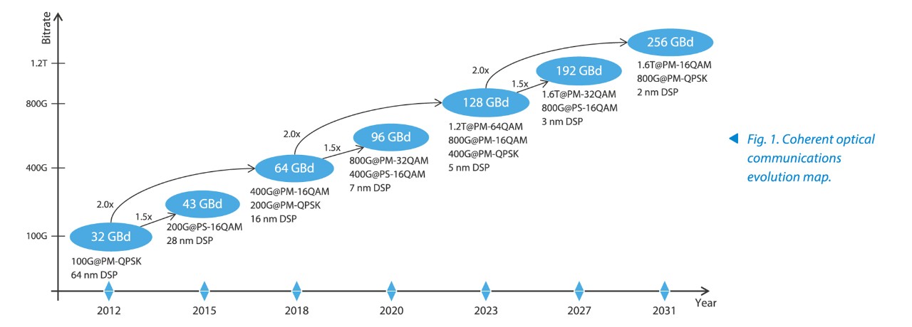
It can be seen from Fig. 1 that one generation of coherent optical modules are developed every three years based on the timeline of advanced digital signal processor (DSP) technologies and the rule of baud rate evolution. The coherent 96 GBd technology began to enter the market in 2020. It uses PM-32QAM modulation signals and ultra-strong forward error correction codes to achieve coherent 800G transmission. The coherent 128 GBd technology is expected to enter the market in 2023.

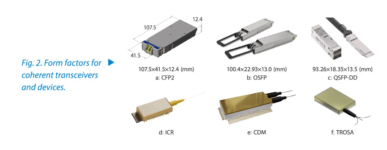
The trends of ultra-high-speed coherent optical module technologies include selection of 128 GBd, band extension to maintain 80-wavelength capacity, and small form-factor pluggable module. According to the OIF 800ZR project, coherent 800G short-distance transmission uses 120 GBd PM-16QAM modulation. Both 96 GBd PS-16QAM and 128 GBd PM-QPSK can implement coherent 400G transmission. The transmission performance of 96 GBd PS-16QAM is not as good as that of 128 GBd PM-QPSK. Without the help of a distributed Raman amplifier (DRA) or G.654.E fibers, 96 GBd PS-16QAM can not meet the transmission requirements of backbone networks over 1000 km. Therefore, the 128 GBd technology will be the mainstream rate of next-generation coherent optical communication after 64 GBd. 75 GHz channel spacing is used for 64 GBd coherent optical transmission, while 150 GHz channel spacing for 128 GBd coherent optical transmission. To maintain the 80-wavelength channel design, the working band of 128 GBd coherent optical transmission needs to be extended to the L band. The second generation of C form-factor pluggable transceiver (CFP2) modules are used as coherent optical modules for metro and long-distance transmission. Smaller quad small form-factor pluggable-double density (QSFP-DD) and octal small form-factor pluggable (OSFP) modules are used as coherent optical modules for data center interconnect (DCI) short-distance transmission. Metro and DCI coherent optical modules tend to be integrated. The 800G coherent optical module standard includes the OIF-800ZR project, which is under development. The standardization work of OpenROADM and OpenZR+ for long-distance coherent 800G transmission has not been publicly reported.
Ultra-High-Speed Optical Devices
Key units of a coherent optical module include integrated coherent receiver (ICR), coherent driver modulator (CDM), integrated tunable laser assembly (iTLA) and DSP chips (Fig. 2). Optical devices involve separate and integrated solutions. The separated solution contains independent optical devices such as iTLA, CDM, and ICR. The integrated solution combines the units mentioned above into integrated devices including transmit-receive optical sub-assembly (TROSA) that can be an integration of iTLA+CDM+ICR or CDM+ICR, and multi-chip module (MCM) that can be an integration of CDM+ICR+DSP. Different material technologies are applicable to different packaging forms. MCM has high integration and high performance, but it requires optical chips to support non-hermetic packaging.

Key Technologies
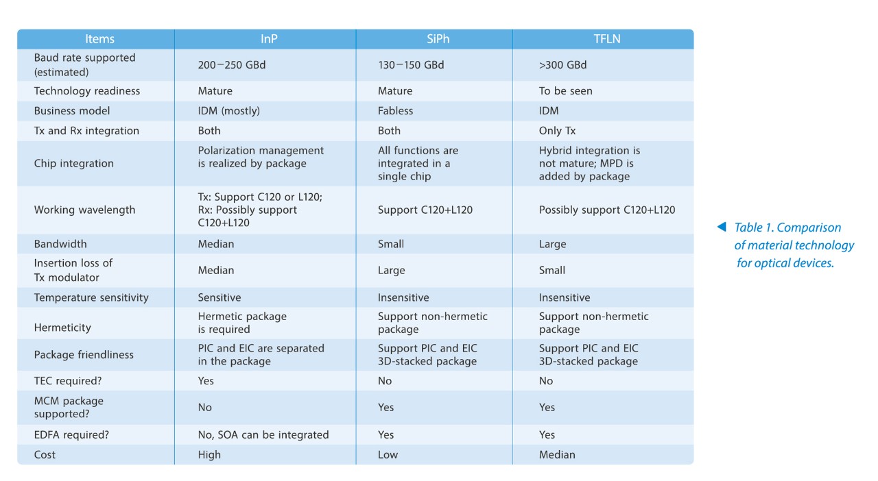
Key technologies of ultra-high-speed optical devices include material technology, wide spectrum band technology, large bandwidth modulation technology and advanced packaging technology. The material technology includes indium phosphide (InP), silicon photonics (SiPh) and thin film lithium niobate (TFLN), as shown in Table 1. InP and SiPh are mature material technologies, while the new material technology TFLN has a promising application prospect due to its outstanding low loss and large bandwidth.

Ultra-high-speed optical devices require the wide spectrum band technology to upgrade optical transmission capacity. The 64 GBd modulation signal corresponds to 75 GHz channel width, while the 128 GBd modulation signal 150 GHz channel width. The working wavelength of the 64 GBd system is C120 (120 channels with 50 GHz spacing in the C band), and the working wavelength of the 128 GBd system is C120+L120. If a multi-mode interferometer is used in the optical chip for optical splitting and combining functions, there is a risk of deterioration in edge wavelength performance, which is a great challenge to the InP solution. The SiPh solution can use a broadband coupler for multi-band operation. The germanium detector in the SiPh solution needs to consider whether the responsivity near the 1626 nm decreases or not. SOA and InP modulators are difficult to implement C120+L120 in a single chip.
The large bandwidth modulation technology is related to optical chip, electrical chip and packaging solution. Using electrical chips to compensate for the bandwidth shortage of optical chips is an effective means to achieve large bandwidth in the photoelectric synergy of ultra-high-speed optical devices. InP and SiPh modulators are limited, so both need to make use of the bandwidth peaking effect of electrical chips of the driver to increase bandwidth. The chip of a TFLN modulator can support a bandwidth of above 100 GHz according to an experiment report.
Advanced packaging technology is related to the optical chip material technology. Shortening the distance of high-speed electrical signal transmission lines and reducing impedance discontinuity have become the trend of packaging for ultra-high-speed optical devices. The MCM packaging with DSP has become a hot topic in R&D. Traditional InP chips need hermetic gold box packaging, such as separate devices ICR and CDM, and the integrated device TROSA. SiPh chips support non-hermetic ball grid array (BGA) packaging. Due to the limited bandwidth of optical chips, MCM is preferred to TROSA. MCM has fewer impedance discontinuity points. In particular, it does not go through BGA solder ball twice, so it has better bandwidth performance and higher integration. The TFLN chip supports both advanced BGA packaging and traditional CDM packaging. If the optical chip does not support the through silicon via (TSV) process, the wire bonding is used, in which high-speed signals need double-wire bonding, and the substrate implements short-distance wire bonding by means of cavity.
Conclusion
The 96 GBd and 128 GBd ultra-high-speed optical devices are key components for building high-performance optical infrastructure. Considering 800ZR standardization and the difference of transmission performance, 128 GBd optical devices are expected to be more widely used.
When the baud rate of the signal increases, it is necessary to expand the working wavelength band to upgrade the capacity of fiber optic transmission. At present, the industry has started to study the technical feasibility of implementing S+C+L+U bands. As the further increase of the signal baud rate poses more and more challenges to optoelectronic chips, multi-channel highly integrated optical devices will also become a trend.